APSS Unique Features(Comparison with Conventional Simulators) |
Circuit Simulator APSS is the only Photonic CAD tool that can analyze complex integrated circuits. Regular methods, such as FDTD, cannot be used to analyze circuits due to its large size. Some circuits contain 90 or 180 degree bends that make them impossible to be used by standard simulators such as BPM. APSS has a specific simulator for photonic circuits. The concept has been well accepted in electronics circuit design, i.e., LSI performance is calculated by small sub circuits which build up LSI. The GUI (Graphic User Interface) of APSS is so powerful and easy to use so designers can easily create any complex circuits. 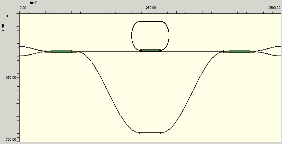 Application oriented rather than method orientedl Unlike other photonic tools that has only one numerical method, such as BPM or FDTD, APSS does not focus on the method. It has all the numerical and analytical methods, and a proper one is selected for a specific design. Take a simple step junction. If user wants to evaluate the transmission, APSS provides BPM. If user also interested in the reflection, APSS uses BPM+FDTD. All setting is embeded in the software, and user can define its own setting to investigate the device performance. Another example could be S-bend, or a Elliptical bend. There are a number of different analytical and numerical methods available for this kind of devices. If the user wants to have a quick estimation of the transmission loss and return loss, 2D analytical method could be selected. That includes:
Complete solution with fully integrated hierarchical framework APSS offers complete design solution from basic selecting materials to the final exporting mask files of a photonic integrated circuit (PIC). To simplify a design work, APSS is designed in a hierarchical framework consists of Material, Waveguide, Device, and Circuit modules according to the current processing technology procedure. This way, a big and complicate design problem can be decoupled into a number of smaller and simpler problems in order to be solved step by step, may by different people with different expertise by different specialized solvers. By modulling the PICs, designers could focus on the separated issues at different stages. Similar to the processing technology, different stage may required different and combined expertise, such material science, processing technology, optical/electromagnetic/RF theories, as well as packaging technology. Therefore, APSS provides an integrated platform for a group of designers can work together on a complex project and a specific module for individual designer to work on a specific problem. It provide a complete solution from basic material to final mask file for PIC designers. Knowledge based with pre-defined libraries To overcome the entrance barrier and shorten the learn curve for new users, all the possible known knowledge is built in those pre-defined libraries and user do not need to read all the details before they can start the design work. This also saves designers' time and effort in creating some of the popular material, waveguide, and devices such as
In addition to those pre-defined libraries, APSS provides a User-defined environment for advanced users to design those waveguides and devices which are not included in the library. General Features Beside the above general features, APSS has several important features which some of them are unique in Apollo software. Some of APSS features are: Material Module
Waveguide Module
Device Module
Circuit Module
|